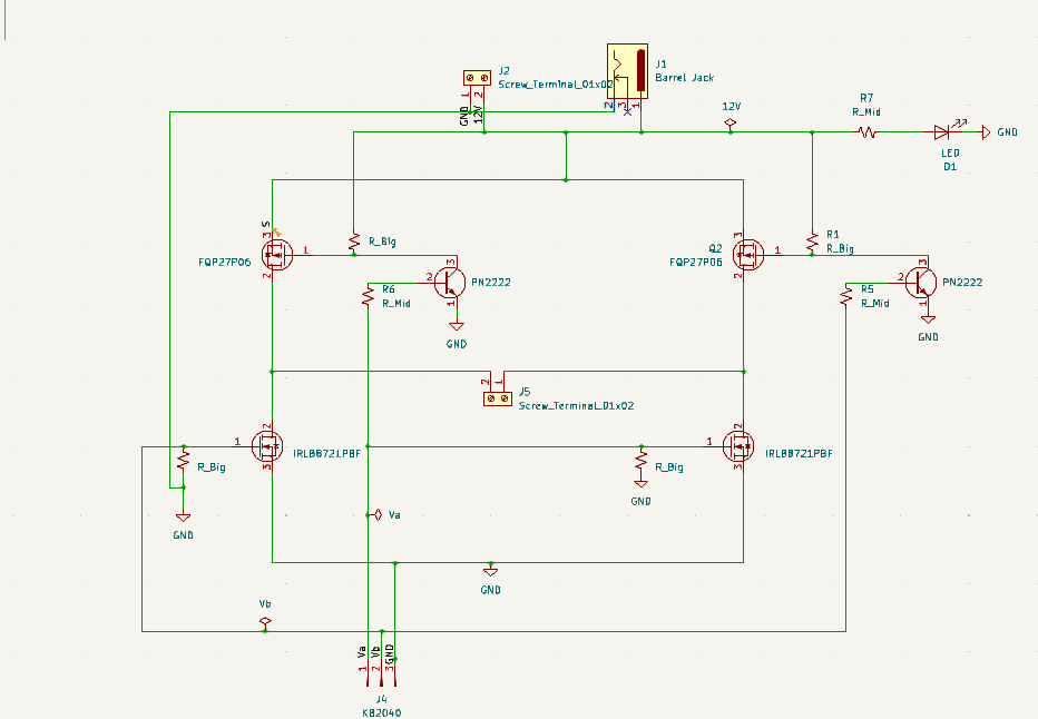
Before I started designing the actual PCB, I first had to create a schematic of the desired circuit. Using KiCad's schematic builder,
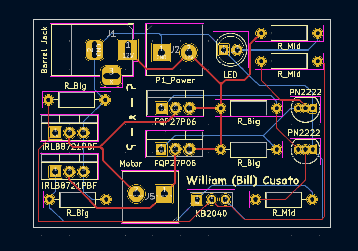
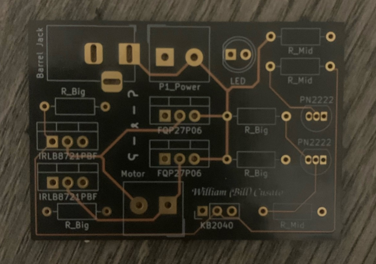
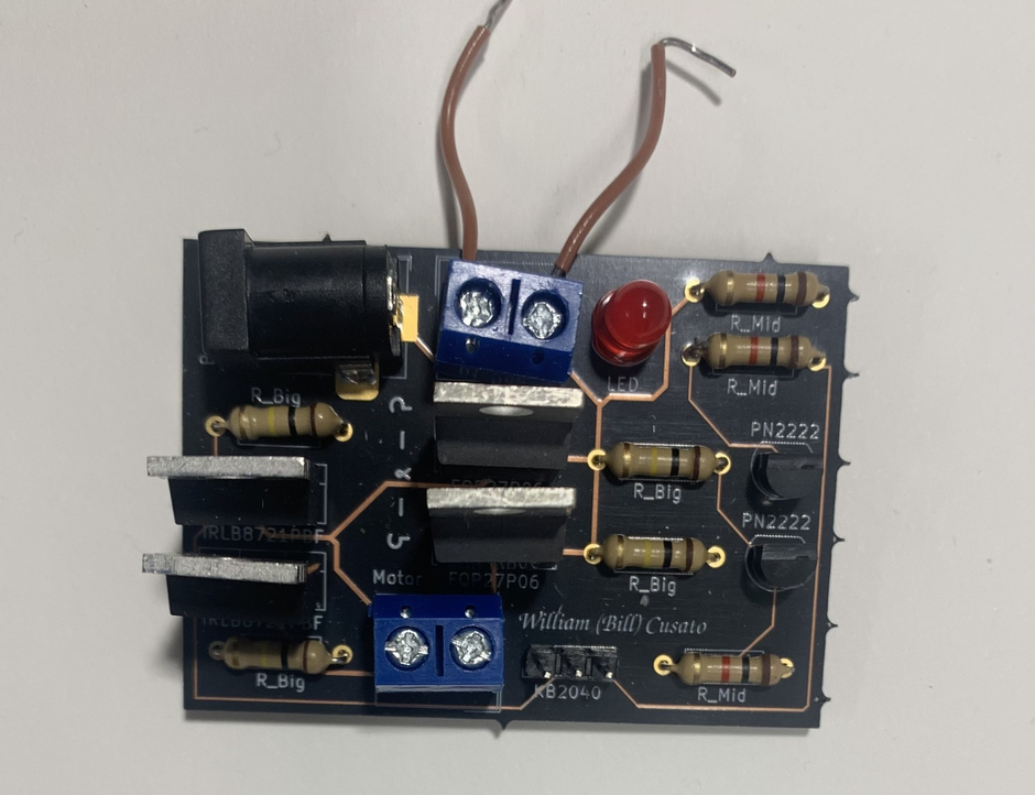
I designed an H-Bridge using N and P-channel MOSFETs as well as NPN bipolar transistors. Then, I imported my schematic into KiCad's PCB designer.
For 'wires' that could carry large currents, I ensured to increase the wire width to prevent them from overheating.
The results of both the schematic and the PCB layout can be seen below.
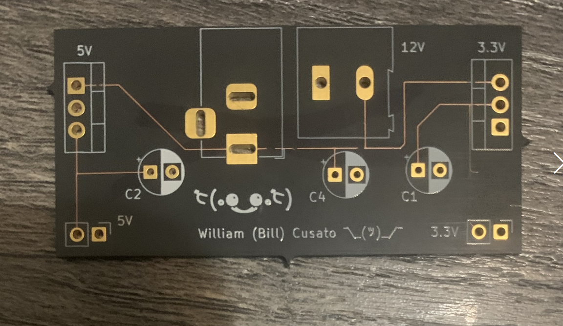
This past semester, I had the opportunity to create a couple of useful PCBs.
The first is a voltage regulator PCB that outputs both 3.3V and 5V. It can be seen to the right (without components attached).
This was my first experience designing a PCB, and I aimed to improve in every aspect for the subsequent H-Bridge PCB!